- 您现在的位置:买卖IC网 > Sheet目录340 > MAX16821CATI+T (Maxim Integrated)IC LED DRIVR HIGH BRIGHT 28-TQFN
High-Power Synchronous HBLED
Drivers with Rapid Current Pulsing
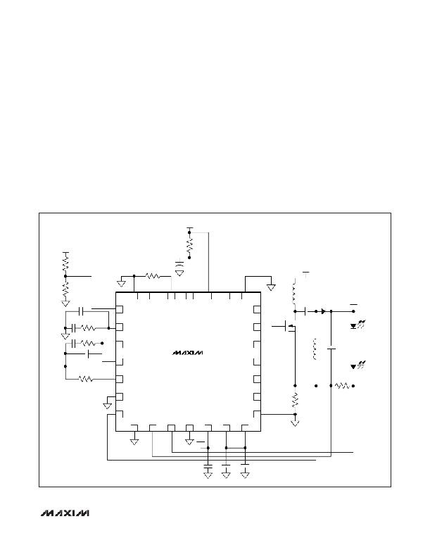
SEPIC LED Driver
Figure 7 shows the MAX16821A/MAX16821B/
MAX16821C configured as a SEPIC LED driver. While
buck topologies produce an output always lower than
the input, and boost topologies produce an output
always greater than the input, a SEPIC topology allows
the output voltage to be greater than, equal to, or less
than the input. In a SEPIC topology, the voltage across
C3 is the same as the input voltage, and L1 and L2 have
the same inductance. Therefore, when Q1 turns on (on-
time), the currents in both inductors (L1 and L2) ramp
up at the same rate. The output capacitor supports the
output voltage during this time. When Q1 turns off (off-
time), L1 current recharges C3 and combines with L2 to
V CC
provide current to recharge C1 and supplies the load
current. Since the voltage waveform across L1 and L2
are exactly the same, it is possible to wind both induc-
tors on the same core (a coupled inductor). Although
voltages on L1 and L2 are the same, RMS currents can
be quite different so the windings may require a differ-
ent gauge wire. Because of the dual inductors and seg-
mented energy transfer, the efficiency of a SEPIC
converter is lower than the standard buck or boost con-
figurations. As in the boost driver, the current-sense
resistor connects to ground, allowing the output voltage
of the LED driver to exceed the rated maximum voltage
of the MAX16821A/MAX16821B/MAX16821C.
V LED
R4
ON/OFF
R8
R3
C2
V IN
7V TO 28V
R9
14
13
12
11
10
9
8
L1
C10
I.C.
OUTV
RT/SYNC
EN
MODE
CLKOUT
SGND
C3
D1
V LED
15 OVI
N.C. 7
C9
R7
16 CLP
DH 6
Q1
R6
C8
C7
17 EAOUT
18 EAN
MAX16821A
MAX16821B
LX 5
BST 4
L2
C1
LED
STRING
R5
MAX16821C
19 DIFF
20 CSN
21 CSP
DL 3
N.C. 2
PGND 1
R1
R2
SGND
22
SENSE-
23
SENSE+
24
SGND
25
IN
26
V CC
27
V DD
28
V IN
Figure 7. Typical Application Circuit for a SEPIC LED Driver
C6
C5
C4
______________________________________________________________________________________
15
发布紧急采购,3分钟左右您将得到回复。
相关PDF资料
MAX16822AASA/V+
IC LED DRIVER HIGH BRIGHT 8SOIC
MAX16826ATJ+C24
IC LED DVR HB PROGR 32-HQFN
MAX16835ATE+T
IC LED DRIVR HIGH BRIGHT 16-TQFN
MAX16838AUP+
IC LED DRIVR HIGH BRIGHT 20TSSOP
MAX1698EUB
IC LED DRVR WT/CLR BCKLGT 10MSOP
MAX17014EVKIT+
KIT EVAL FOR MAX17014
MAX17061AETI+T
IC LED DRVR WHITE BCKLGT 28-TQFN
MAX17061ETI+T
IC LED DRVR WHITE BCKLGT 28-TQFN
相关代理商/技术参数
MAX16821EVKIT+
制造商:Maxim Integrated Products 功能描述:HIGH-POWER SYNCHRONOUS HBLED DRIVER - Boxed Product (Development Kits)
MAX16822AASA/V+
功能描述:LED照明驱动器 2MHz HB w/MOSFET & HSide Crnt Sense RoHS:否 制造商:STMicroelectronics 输入电压:11.5 V to 23 V 工作频率: 最大电源电流:1.7 mA 输出电流: 最大工作温度: 安装风格:SMD/SMT 封装 / 箱体:SO-16N
MAX16822AASA/V+T
功能描述:LED照明驱动器 2MHz HB w/MOSFET & HSide Crnt Sense RoHS:否 制造商:STMicroelectronics 输入电压:11.5 V to 23 V 工作频率: 最大电源电流:1.7 mA 输出电流: 最大工作温度: 安装风格:SMD/SMT 封装 / 箱体:SO-16N
MAX16822AASA+
功能描述:LED照明驱动器 2MHz HB w/MOSFET & HSide Crnt Sense RoHS:否 制造商:STMicroelectronics 输入电压:11.5 V to 23 V 工作频率: 最大电源电流:1.7 mA 输出电流: 最大工作温度: 安装风格:SMD/SMT 封装 / 箱体:SO-16N
MAX16822AASA+T
功能描述:LED照明驱动器 2MHz HB w/MOSFET & HSide Crnt Sense RoHS:否 制造商:STMicroelectronics 输入电压:11.5 V to 23 V 工作频率: 最大电源电流:1.7 mA 输出电流: 最大工作温度: 安装风格:SMD/SMT 封装 / 箱体:SO-16N
MAX16822BASA+
功能描述:LED照明驱动器 2MHz HB w/MOSFET & HSide Crnt Sense RoHS:否 制造商:STMicroelectronics 输入电压:11.5 V to 23 V 工作频率: 最大电源电流:1.7 mA 输出电流: 最大工作温度: 安装风格:SMD/SMT 封装 / 箱体:SO-16N
MAX16822BASA+T
功能描述:LED照明驱动器 2MHz HB w/MOSFET & HSide Crnt Sense RoHS:否 制造商:STMicroelectronics 输入电压:11.5 V to 23 V 工作频率: 最大电源电流:1.7 mA 输出电流: 最大工作温度: 安装风格:SMD/SMT 封装 / 箱体:SO-16N
MAX16822BEVKIT+
功能描述:LED 照明开发工具 MAX16822B Eval Kit RoHS:否 制造商:Fairchild Semiconductor 产品:Evaluation Kits 用于:FL7732 核心: 电源电压:120V 系列: 封装: